
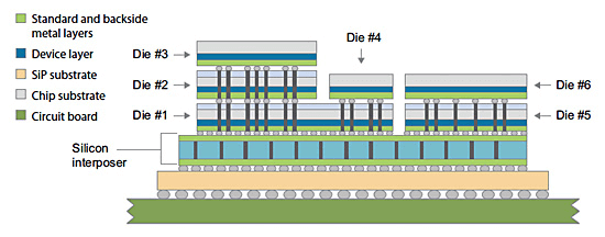
3D IC (3D Integrated Circuits) is a metal-oxide-semiconductor Integrated circuit that is manufactured by the process of stacking silicon wafers and getting them connected in a vertical manner. The connection is achieved either by TSVs or connections such as the Cu-Cu. The main purpose of making 3D IC is to achieve improvements in performance that will work to reduce power and have a smaller footprint as compared to the conventional processes.
BENEFITS OF THE 3D INTEGRATED CIRCUITS:
While the signal propagation speed is improved by the scaling processes of the CMOS, it is becoming more and more costly to scale from the manufacturing and chip design processes in the current scenario. the power density constants are partly responsible for this and another reason would be because the transistors become faster while the interconnects do not. The three-dimensional integrated circuit tries to solve this problem by stacking the two dies for connecting them and giving them a three-dimensional figure. This is very effective in speeding up the communication as compared to the planar layout.
The various advantages that the 3D Integrated circuit offers over the traditional planner layout are:
- Shorter Interconnect: Using the 3D model, the wild introduces by 10% to 15% thus reducing the average length of the wire that is used. Although this change is very small, the effect can be seen prominently in longer interconnects, which affect the circuit delay by a great amount. if you consider that 3D wires have capacitance very high then the improvement of circuit delay is not guaranteed.
- Higher Bandwidth: 3D integration allows a very large number of vertical connections between the 2D layers. This feature of the 3D Integrated circuit allows for the construction of buses with a wide bandwidth between the functional blocks that are present in different layers. We can take the example of a processor plus memory 3D stack that has its caches stacked on top of the processor. This allows us to have a much wider bus than it typically has And this will also give a solution for the memory wall problem.
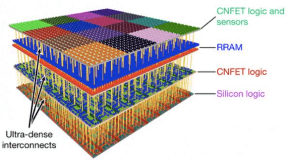
- Heterogeneous Integration: 3D Integrated circuit is much more optimizable because it can be built with different processes and even different wafers. This makes the circuit much more optimizable than if it was built on a single wafer. Furthermore, the components from different manufacturers could be combined in a single circuit.
- Design and Power Efficiency: The additional dimension not only gives us a higher level of connectivity but also offers various new possibilities in the design of the Integrated circuit. Due to the design, the circuit uses shorter wires that also reduce the consumption of power that is caused due to the parasitic capacitance. The three benefits that we get out of this are a reduction in heat generation, lower cost of operation, and extended battery life.
- Circuit Security: The stack structure of the 3D IC makes it very complicated for being reverse engineered. It helps achieve security through the method of obscurity. Layers are divided in such a way that the data is obscured at each layer. Moreover, the design allows the separate layers to have their own system monitor features. This makes the 3D IC more secure than the traditional one.
CHALLENGES OF THE 3D INTEGRATED CIRCUITS:
This technology is relatively new and is still under development and research. Thus it has a few drawbacks just like all developing technologies.
- Cost: The commercialization of the 3D ICs in the mainstream consumer application has been very challenging. What has been put for addressing this issue such that it can be scaled to a point that it can be profitable. The manufacturing cost of the 3D IC can be easily broken down into its stages of manufacture despite being such a new technology. After breaking down the cost in stages, the cost drivers can easily be identified and once they are identified, it can be easily defined where the majority of the cost is coming from and how it can be reduced.
- Testing: Testing of the individual layers is very important if we want to achieve a high yield overall and reduce the cost. But due to the design of the 3D IC in which the adjacent layers are tightly interconnected, it becomes very difficult to test the individual layers separately. Due to being a 3D model, its circuit cannot be tested by conventional means thus incurring additional overheads.
- Few Standards: Very few standards exist for the 3D IC model in its manufacturing, designing, and even packaging. Although this issue has been already addressed, very few actions have been taken to solve this issue. The use of heterogeneous integration supply chain is that the delay caused by the supplier of a particular part causes a delay in the delivery of the whole product. This in turn causes delays in the revenue generation of each product.
- Yield: As we know every step in manufacturing adds a chance of defect in the product. If we want the product of 3D IC to be viable on a commercial basis, the defects that are caused should be repairable or tolerable. The otherwise public commercial application would be very costly.
- Heat: The 3D IC is in the form of a stack. In the design of a stack, heating is an inevitable issue because the electrical proximity greatly correlates with thermal proximity. So the heat that builds up must be dissipated and the thermal hotspots that exist in the structure must be managed carefully.